There are few products that require as many production steps as semiconductor manufacturing. The production processes in this industry are intricate and involve hundreds of different steps, which makes the implementation and coordination of processes correspondingly complex and sensitive. This calls for technologies that can be used and adapted quickly while at the same time boosting production efficiency. Machine vision plays a key role here. It enables the numerous inspection and alignment processes required in high-precision semiconductor production to be carried out automatically and accurately. Robust machine vision software is used to implement applications such as defect detection, measurement, as well as matching and alignment, which provide significant advantages at various production stages.
In nearly every production scenario in semiconductor manufacturing, at least one step involves checking whether the product has functional or optical defects. Using machine vision to perform this quality control automatically offers numerous advantages over manual inspection:
Machine vision is much faster, the results are objective and reproducible, and the quality of the inspection does not run the risk of deteriorating due to fatigue or the monotony of the task.
Deep learning technologies add a little something extra for this purpose. For example, deep-learning-based anomaly detection enables automated surface inspections, including identifying defects and providing the foundation for subsequent defect segmentation – applications that previously were simply impossible. In terms of quality control, determining the dimensional stability is just as essential as detecting defects. Machine vision makes it possible to measure edges along lines or circular segments with subpixel accuracy in a matter of milliseconds. In addition, 3D measurement methods enable the reconstruction of disparity images, distance images, or 3D surface coordinates using advanced techniques.
Apart from quality inspection, finding and aligning wafers and chips is another application in which machine vision can provide very effective support. This primarily involves the use of subpixel-precise shape matching. The technology finds objects precisely and robustly in real time. This works even if they are rotated, scaled, distorted in perspective, locally deformed, partially obscured, or outside the image.
Roughly speaking, the production process for semiconductors is divided into frontend and back-end production. During front-end production, chemical and physical processes are applied repeatedly to a substrate, i.e., a wafer, in order to build micro-electronic circuits layer by layer. The individual wafers are then separated in the back-end production, contacted, fitted with a housing, and prepared for use. Machine vision offers a wide range of technologies that can be used in numerous process steps in both front-end and back-end production. Let’s start with the front-end production. Machine vision’s key application – as well as its specialty – is defect detection, for example the robust detection of a wide range of defects on the surface of a wafer. Machine vision technologies identify microscopic cracks, scratches, and particle contamination on the wafer surface, even in difficult lighting conditions. This can involve the use of various technologies, such as deep-learning-based anomaly detection, or a “conventionally” trained variation model.
In order to achieve maximum speed and performance, a combination of rule-based algorithms and AI methods is often recommended.
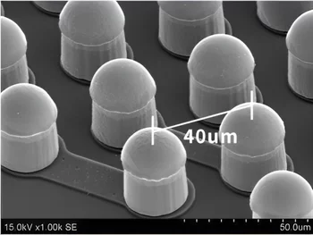
Another example in front-end production is the measurement of what are known as wafer bumps. These are protruding, metallic solder balls that are attached to the wafer. The bumps provide the connection between the chip and the circuit board, for example. Their precise height, diameter, and the overall uniformity of the structures are vital to ensure flawless functionality and reliability. Three-dimensional image processing technologies, such as 3D surface inspection, shape-based 3D matching, and 3D measurement, can be used to inspect and measure these bumps accurately.
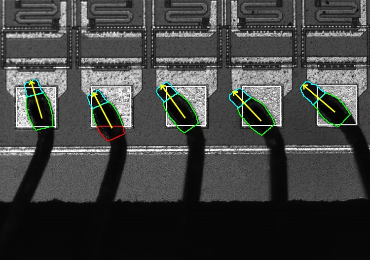
There are also great examples of how machine vision can support back-end production. One application is wire bonding, i.e., attaching the connecting wires between the semiconductor and the housing or other components. Bond inspection is a proven quality control process, especially when packaging the chip. It requires utmost precision to evaluate the position of the wire and the integrity of the bond at a microscopic level. Machine vision technologies used for this are measurements with subpixel accuracy in 2D and 3D. They reliably detect the slightest gaps and deviations in position, even against of complex backgrounds. This makes it possible to create cross-section profiles along the local axis direction, for example, which enables detailed analyses. There are many other examples of how cutting-edge machine vision technologies, such as those from MVTec, are optimizing semiconductor manufacturing. However, the editors of this magazine have not given me enough space to elaborate any further in this article. For more information, please refer to the adjacent information box and QR code.