Machine vision and AI increase throughput, stabilize processes, and help manufacturers meet strict quality and yield requirements, even at high line speeds and submicron structures. They also reduce unplanned downtime by detecting defects or misaligned wafers before they can block, damage, or stop equipment.
Typical machine vision tasks
enabled by MVTec software
DEEP OCR & 2D CODE READING
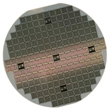
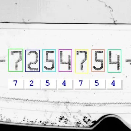
Wafers must remain uniquely identifiable throughout the entire production process. Typical markings include batch numbers, dates, manufacturer codes, and other process information.
MVTec's Deep OCR and code reading technology reliably reads characters and 2D codes even under challenging lighting, low contrast, or variable marking quality. Automatic grouping of characters into words improves recognition accuracy and reduces misreads of visually similar characters – for example, in wafer sorters and Equipment Front-End Modules (EFEMs).
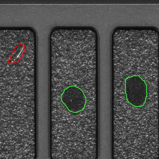
DEFECT DETECTION
Scratches, micro-cracks, and particles directly impact yield and machine reliability.
MVTec software combines rule-based image processing with deep learning-based methods like anomaly detection to detect all kinds of defects on wafers, dies, and packages.
The software delivers robust results even on highly structured or noisy backgrounds and supports high speed and semiconductor equipment.
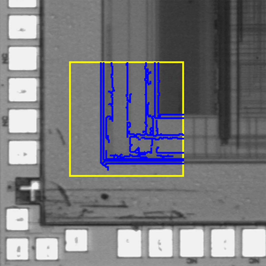
2D/3D METROLOGY
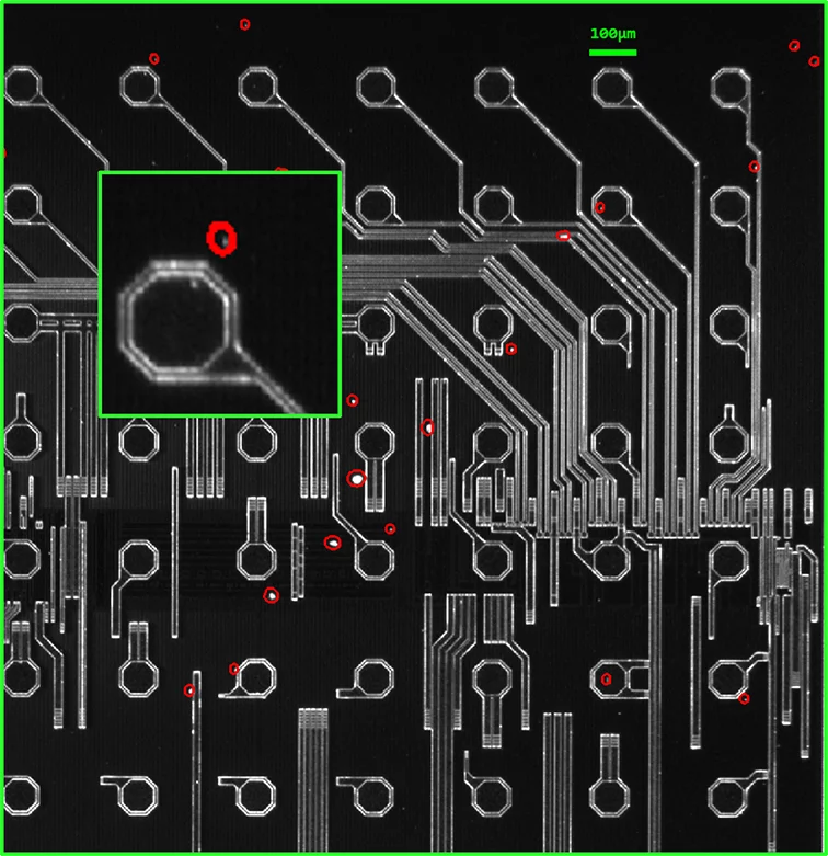
Redistribution layers (RDL) are critical for interconnects between chips and substrates. Their geometry must be inspected in the micron range to ensure compliance with design rules. MVTec provides subpixel-accurate pattern matching and metrology methods for precise alignment and 2D structure measurement down to 1/50 pixel. The flexible toolbox approach enables users to select the best combination of algorithms for each inspection setup and object.
Image source: Sawyer, Brett, Yuya Suzuki, Zihan Wu, Hao Lu, Venky Sundaram, Kadappan Panayappan, and Rao Tummala. 2015. “Design and Demonstration of 40 Micron Bump Pitch Multi-Layer RDL on Panel-Based Glass Interposers.” IMAPSource Proceedings 2015 (1): 379–85. https://doi.org/10.4071/isom-2015-WP24
3D VISION
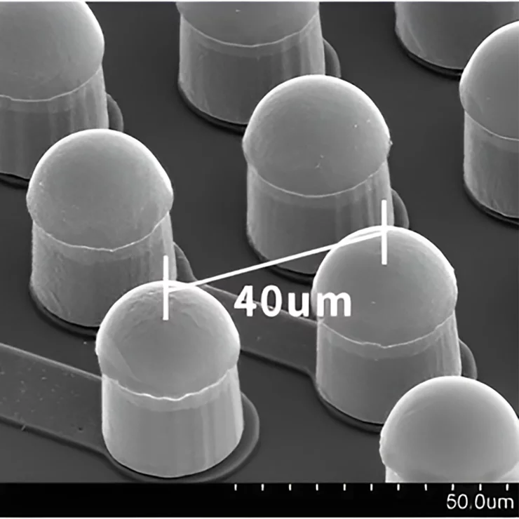
Advanced packaging requires highly accurate bump structures for reliable electrical interconnects.
MVTec's 3D vision toolset supports surface-based 3D matching, 3D object processing, and 3D surface inspection for bump geometry and coplanarity checks. It handles data from various 3D sensor technologies, including electron microscopy, and provides high-speed, high-accuracy 3D metrology. Even arc and spherical surfaces can be reconstructed and analyzed precisely.
Image source: arthasarathy, Ravi, and Umut Tosun. 2023. “Defluxing of Copper Pillar Bumped Flip Chips.” IMAPSource Proceedings 2023 (DPC): 438–82. https://doi.org/10.4071/001c.90768
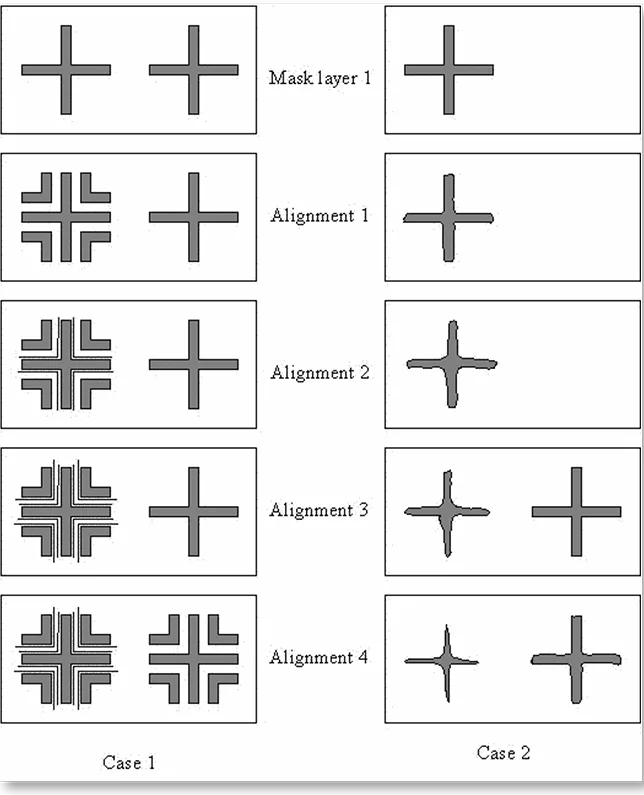
PRECISION ALIGNMENT
Shape-based matching aligns the current wafer position to existing patterns by precisely calculating displacement and rotation.
The orientation of the wafer can be derived from a single image. Operators in our software HALCON estimate rotation angles and ensure correct alignment before critical steps like probing or pick-and-place.
POSITION RECOGNITION
Precise positioning and bonding are essential for reliable electrical connections.
MVTec software provides subpixel-accurate 2D and 3D measurements and detects small positional deviations or voids, even in complex backgrounds. Cross-section profiles along local axial directions allow detailed bond analysis.
MVTec Software

MVTec combines classical rule-based algorithms with AI methods such as deep-learning-based classification, segmentation, and anomaly detection. This enables: