Success Story
As energy prices continue to rise, the call for regenerative energy sources is growing louder. One of the fastest growing sectors among them is photovoltaics, in other words the generation of electric power from solar energy. Rapid technological progress has contributed to the fact that a widespread use of solar thermal systems is becoming increasingly affordable. Government funded projects, such as the German "100,000 Roofs" program, additionally stimulate the solar market. The key criterion in the use of solar modules is their efficiency factor. To achieve maximum power output, high demands are placed on the quality of each wafer produced for solar cells. The German company ECKELMANN AG meets this challenge with a newly developed wafer inspection system. High-resolution Gigabit Ethernet cameras from IDS and a powerful image processing application form the backbone of this system.
The solar energy that reaches the Earth's surface is up to 1,000 watts per square meter. Extrapolated to the whole globe of the Earth, this energy is equivalent to more than 10,000 times the global annual demand for primary energy. The actual challenge is to make the best possible use of this potential. Solar cells are usually made of polycrystalline silicon, which is complicated and therefore expensive to manufacture. The efficiency, i.e. the amount of solar energy converted to electric power, should be as high as possible. However, the theoretical maximum of 30% is far from being reached even under laboratory conditions. For the manufacture of the about 0.2 mm thin raw silicon wafers, this means exacting demands on purity and freedom from defects. Frequently occurring manufacturing defects that would cause power loss in the solar module include chipping, cracks and broken edges in the wafers. Digital image processing using high-resolution cameras proved the only viable way to ensure early detection of these defects. Manual quality assurance is next to impossible as the fragile wafers are difficult to handle – even more so at the high throughput rates required for production.
The Image Processing and Intralogistics department at ECKELMANN is currently developing a new test and inspection station for a customer who wants to equip several wafer production lines with the system. The production lines have a throughput of 3,600 wafers per hour. This leaves the station just about a second to not only inspect a wafer for flaws, chipping and edge defects, but also to measure the wafer's surface area and the angle of each chamfered corner. When the test and inspection station will be finished, more than two man-years of development work will have gone into camera control and image processing. "The trickiest thing has been to get the necessary accuracy at that fast throughput rate," summarizes Jan Helmerichs, one of the software developers in charge of the project. The work paid off: With the combination of a large field of view paired with high measurement accuracy and a fast throughput time of 0.8 sec, the German company estimates to have taken the lead over competitors.
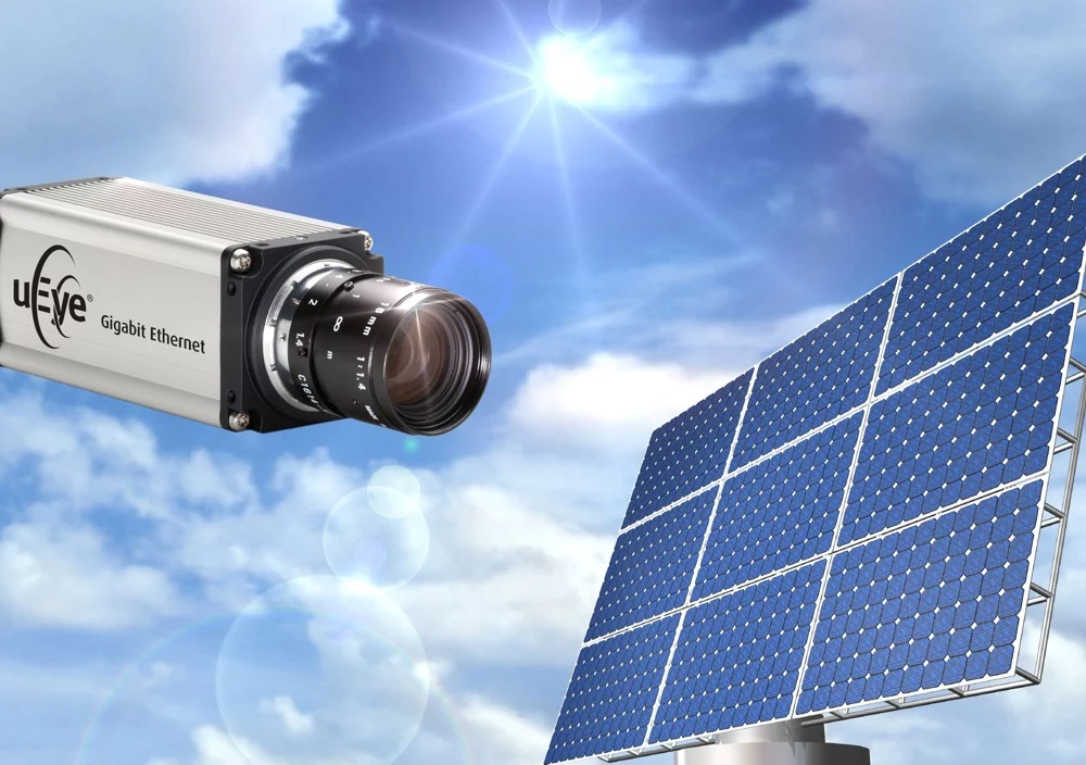
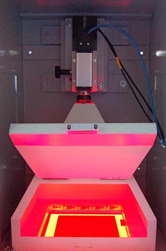
The system needs to achieve a measurement accuracy of 50 µm. To be able to capture images of the approx. 150 mm x 150 mm standard wafer size at the required resolution, the developers opted for a camera with a 5 MP sensor. Project manager Johannes Stelter lists the key criteria: "High resolution, fast and easy image transmission, color." Based on previous good experiences with camera integration, product quality, service and support from IDS, he decided on a model from IDS's uEye series. The UI-5480-C has a high-speed CMOS color sensor with 2560 x 1920 pixels and an area of interest (AOI) function for limiting the field of view to a square partial image. The image data are transmitted at high speed through the camera's Gigabit Ethernet port, resulting in a frame rate of 15 frames per second at full resolution. Cable lengths up to 100 m allow a flexible positioning of the camera even at a large distance from the host computer. In the new wafer inspection station, the camera is installed in a metal housing that is open at the bottom and has built-in lighting. During production, a rotary table positions the sawn silicon wafers below the camera for in-line inspection. The camera takes two successive images, each with different lighting.

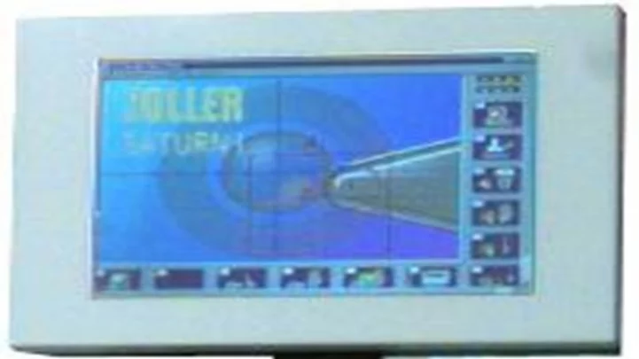
First the wafers are examined in red LED backlight to make through-cracks visible. While the camera takes the second image, the analysis software based on MVTec's HALCON is already segmenting the first image using grayscale operators. As image capture and analysis can be performed in parallel, this solution saves valuable time. The second image is taken using incident white light. Impurities and defects on the surface as well as non-throughgoing cracks contrast clearly under the diffuse LED lighting. This image is also used for measuring the wafer size and the chamfers at the corners. The measuring system can be operated either locally or remotely through the graphical user interface E.SEE-Waferinspect developed by ECKELMANN. The modular system can be expanded by additional measurement functions such as wafer thickness and grain size, according to customer requirements. The corporate philosophy is to flexibly customize standard components to the individual customer's needs. Consequently, the cameras have to not only meet the technical specifications, but yet another essential requirement: easy integration and expandability. Here is where the uEye demonstrates true excellence through the software development kit (SDK) that ships with every camera. The uEye SDK provides a ready-to-go interface for the HALCON software library that is used in the wafer inspection system. This greatly facilitates integrating the camera with the analysis program and ensures that all important functions are available. Besides interfaces for ActiveX, DirectShow and various libraries, the uEye SDK also features a direct programming interface (API) for accessing the driver in C++, C# and VB, for example. More than 20 ready-to-run sample applications complete with source code make it easy to get started with camera programming. Another major advantage is that all cameras of the uEye series use the same SDK, no matter whether they are USB or GigE based. Therefore no programming is necessary in order to switch to a different camera model. And that is an essential aspect in a future-oriented technology like photovoltaics, where it is important to be well prepared for any future requirements.
Author: Daniel Seiler, IDS Imaging Development Systems GmbH ECKELMANN AG is an MVTec Certified Integration Partner.
All product names, trademarks and images of the products/trademarks are copyright by their holders. All rights reserved.