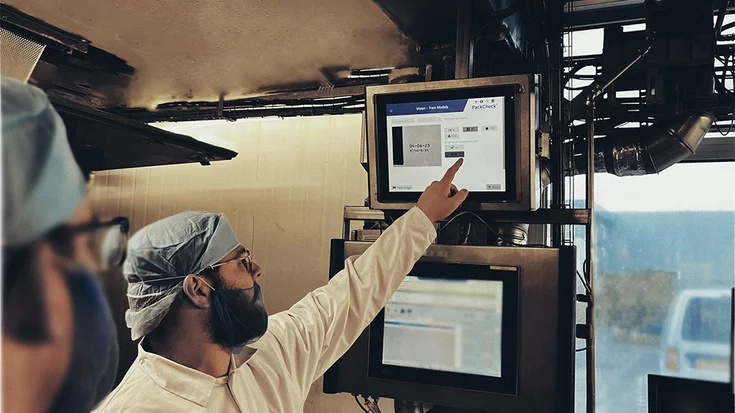
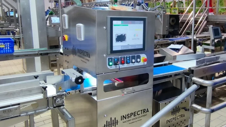
Discover how machine vision enhances efficiency and reduces costs across industries, from agriculture to pharmaceuticals.
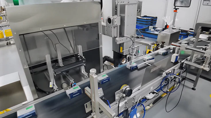
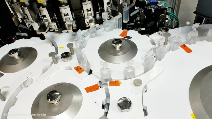
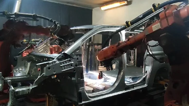
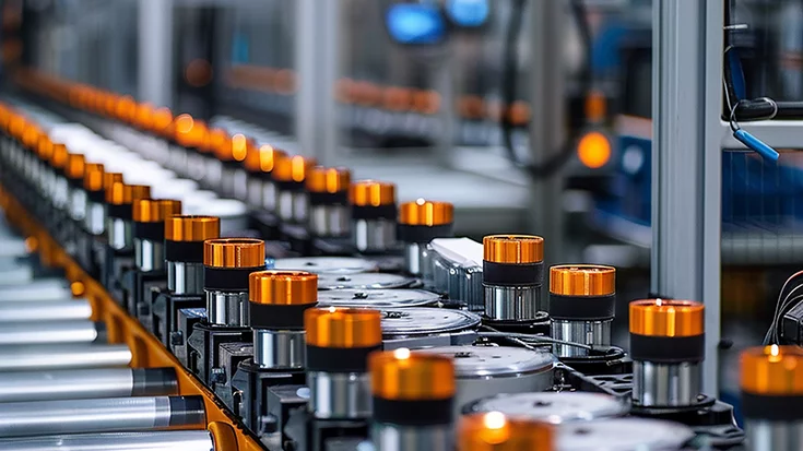
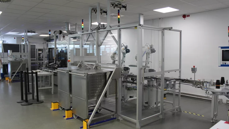
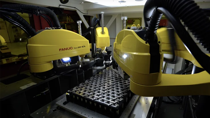
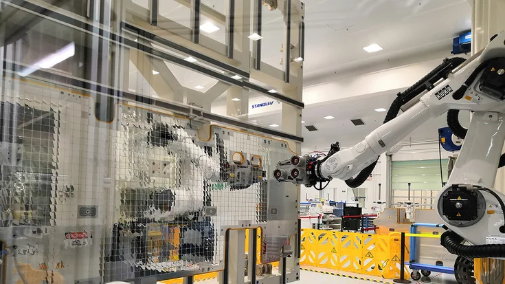
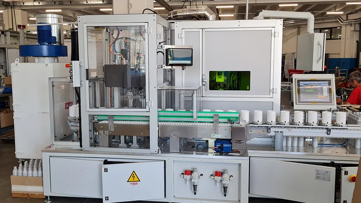
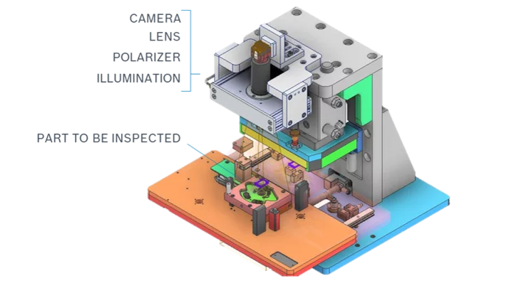
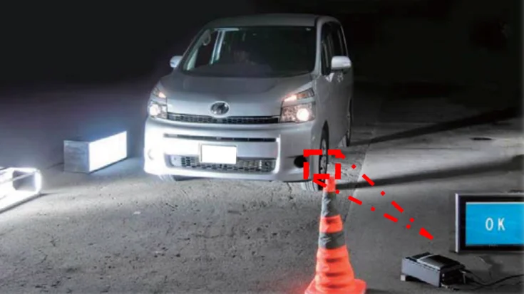
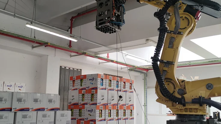
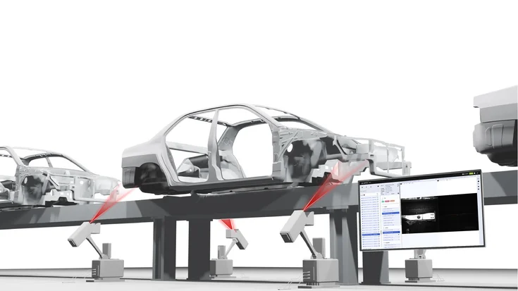
As a multipurpose technology, machine vision is not just limited to individual industries. Especially in modern production scenarios of the Industrial Internet of Things (IIoT aka Industry 4.0), almost every company can benefit from machine vision for cost reduction and optimization of processes.